Large size 12″ wafer laser marker handler
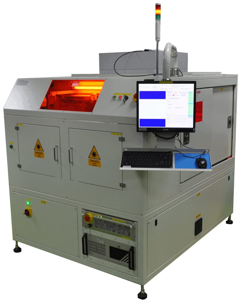
This machine was developed for multiple sizes wafer marking and handling. The wafers are loaded in cassettes into the machine. There are two ports for concurrent processing of one port while loading/unloading of the cassette in the other port. Some of the features:
- Class 1000 cleanroom
- Two cassette dual port load/unload operation
- Anti static materials construction and anti static blower
- High accuracy marking
- Proven wafer ring transport and handling mechanism
- CIM communication to host
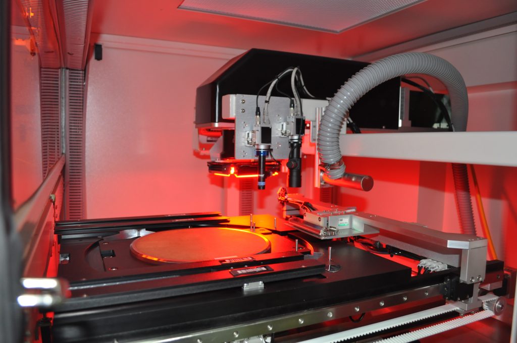
Click on link to view brochure
LN dual laser robot wafer marker
This wafer laser marker is for a special material which normal laser wavelength would penetrate instead of being coupled to the LN material. So a special wavelength laser marker is required. The machine can accept both 6″ and 8″ wafers. Dual laser markers are implemented to save on machine footprint. Dual forks are designed in to reduce wafer transfer time to a minimum.
Chip scale packaging wafer laser marking
With the widespread adoption of CSP technology and the increasing drive towards miniaturisation there is a need for accurate marking to chip level. Some processes require wafers to be sawn while attached to blue tape on wafer ring. The isolation allows 100% test probing and characterisation of each chip. After test there is a need for immediate marking to prevent product mixing. The mark data can be according to wafer map information obtained from the host or derived locally. Communication with the host can be by SECS GEMS or other public or private protocols.
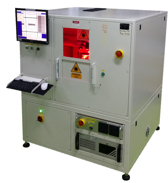
The difficulty in this situation is the slight drift of the chips after saw due to the flexible nature of the blue tape. Using global registration marks are not sufficient when the device size gets smaller down to 0.3 mm x 0.3 mm square. With a need to mark 3 rows of text with character height of 50 um there is less than enough gap between rows and tight tolerance for package drift. Using Scanvision technology to capture the zoom-in image of each chip, the drift can be derived using vision processing and the marking position adjusted accordingly. As an added bonus the marking can be captured again and vision checked for good quality. Rejects can be remarked with another pattern for easy identification.
The software includes special algorithm to handle broken wafers or missing chips. It does this with the help of the wafer map obtained from the host and built-in knowledge of each wafer type ideal shape. This feature is important to ensure perfect accountability and can even be used to countercheck and update the host information on the current situation of each wafer in the assembly line.
All this is done at high speed to ensure high machine throughput. As the registration is done by a through-the-lens method there is no requirement for accurate wafer transport XY stages. High speed movement of the XY stages is not required too as the images are captured by light reflecting off galvanometer mirrors.
At such small character size UV lasers are commonly used to achieve very small line width. The right laser type, operational mode, PC to laser signal interfacing method and scanhead control is extremely important to produce the best result to meet this stringent conditions. With many years of experience and knowledge of the best available technology in the market Hylax is able to provide an outstanding solution to this industry.
Machine design includes laser type selection, lighting method, optics path configuration, software customisation to meet user interface needs, host communication, material handling design and many other areas to ensure that each customer receives the best and optimum solution. Besides machine’s performance, Hylax has through the years learnt to put much emphasis on machine reliability. To this end much effort is devoted to simplifying mechanical design and choosing components of proven ruggedness and quality. As reliability is only as good as it’s weakest link no skimping is worthwhile to save a few dollars.
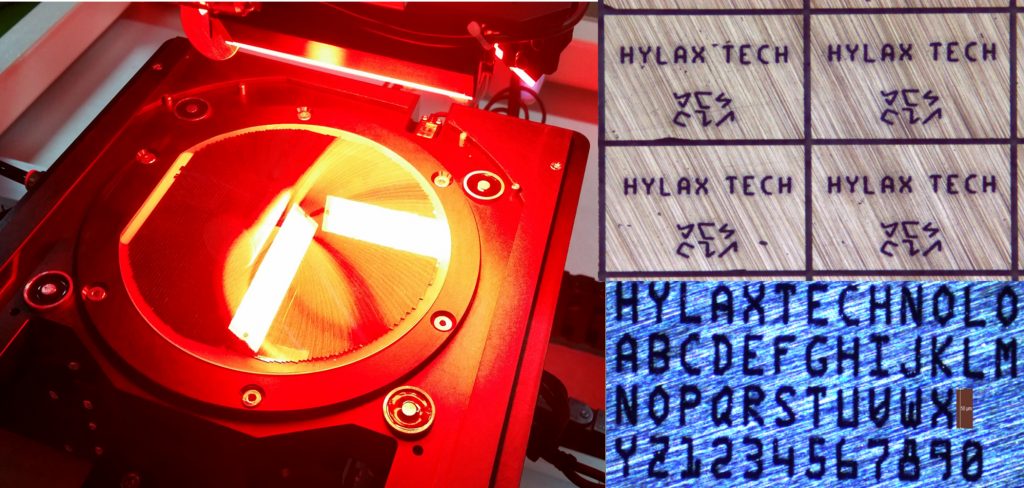
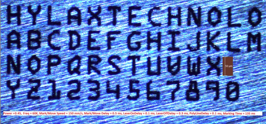
Hylax Technology wafer marker system integrated with the proprietary technology Scanvision pushes the marking technology to the next level of accuracy even with sawn wafers. It is capable of achieving mark landing accuracy of +/-15um and with the mark line width of <10um, it is able to achieve a small character size of 50 um x 50 um. In the above sample the die height is 300 um and there are 3 rows of 50 um height markings. The mark for each die is verified after marking.
Semicon wafer and substrate plate/tile handler
Click on link to view brochure
Simple low cost wafer marker
For low volume wafer production operations like in a company startup stage we can provide a simple stand alone laser wafer marker which can perform all the required marking requirement at a lower price. This setup can be designed to be later integrated into a fully automated machine like the ones shown above.
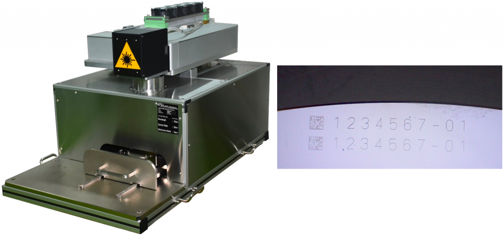
Click on link to view brochure
Wafer ring blue tape laser marking
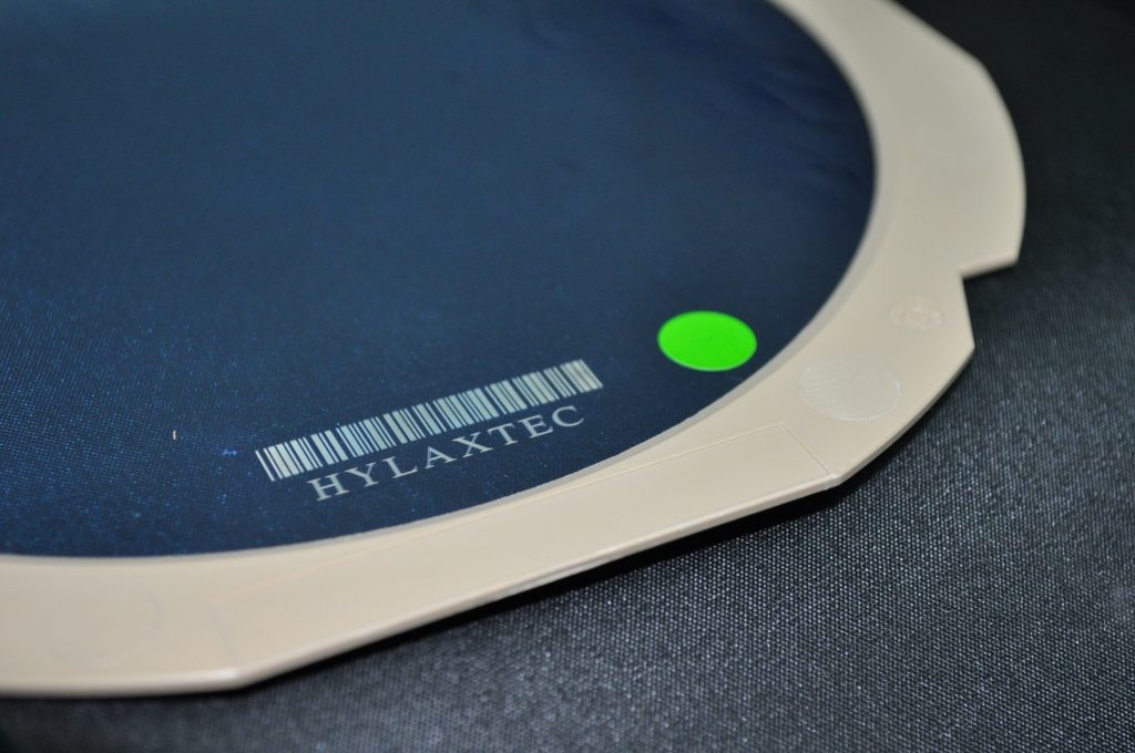
Another break through in the laser application allowing wafer manufacturing to have a more robust traceable marking labels during their manufacturing processes. With this new approach, the laser is marking directly on the wafer film and replacing the traditional stickers method where at times might be lost or damage during the wafer processes. Please contact us today to discuss your requirement.


